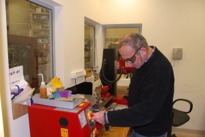
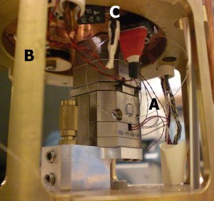
The lab is fully equipped for currying experiments end-to-end, starting from design, through fabrication and ending with measurements and data analysts.
Fabrication
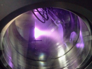 Our group is skilled with various micro and nano fabrication techniques.
Photolithograpy is done in the Technion’s MNFU clean rooms , allowing reproducible micrometer sized features. Elements having dimensions below 1 micron can be fabricated using Electron Beam Lithography (EBL) . We have 3 writing EBL microscopes which were adapted by our group to serve as large area e-beam writers with submicron resolution. In addition we use MNFU’s E-Line writing EBL system and Focus Ion Beam (FIB) system, both of which are capable of reproducing features with resolution down to 10nm.
The group owns several deposition systems for material application. Our RF magnetron sputtering system deposits superconducting materials such as aluminum, niobium and niobium nitride. We also own two evaporation systems for the deposition of other metals (Au,Ti,Ag,Cr) and isolators (SiO2). We use a Reactive Ion Etching Electron Cyclotron Resonance (RIE-ECR) and an Ar ion milling systems for material etching.
Measurements
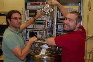 Most of the experiments in our lab are done in a cryogenic environment, i.e at low temperatures. The collection of cryostats in our lab (including wet, i.e. liquid Helium based systems, and dry, i.e. close cycle based cooler) allow measurements at temperatures down to 0.01 Kelvin, with magnetic field up to 11 Tesla.
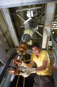 Measurements in the microwave band can be performed with frequencies up to 20 GHz and in the optical band near the wavelength of 1550 nm.
